
Introduction
In 2025, quantum computing will become more of a reality than a possibility. Microsoft’s Majorana 1 quantum chip and ultra-compact optical CMOS quantum devices have brought about major advancements in the development of real-world applications for quantum computing. This article deals with how Majorana 1 & optical chips are forging quantum resources toward real applications. It stands clear that both are rapidly and highly pushing the theatre forward.
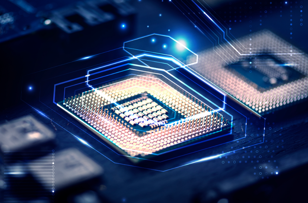
What Is Majorana 1?
The Majorana 1, Microsoft’s first topological quantum processor, was introduced in February 2025. This chip utilizes a topoconductor, made of indium arsenide and aluminum, to establish exotic Majorana zero modes (MZMs) in which intrinsically fault-tolerant qubits form hardware-level resistant errors. According to Microsoft, Majorana is expected to scale up to a million qubits and thus represents a giant leap forward for practical quantum capability.
What Are Optical CMOS Quantum Chips?
Research has recently been completed by Boston University, UC Berkeley, and Northwestern in combining photonics and electronics using microring resonators, producing a 1 mm square slice that incorporates a quantum light factory onto a CMOS chip. A new generation of photonics will help mass-manufacture quantum hardware.
Why These Two Technologies Matter in 2025
Quantum computing has been confined to the realms of laboratory experimentation. Come 2025, both Majorana 1 & the optical chips will bring in new power and scalability:
- Topological qubits offer reduced error rates and increased scalability with Majorana 1
- The ability of the current microchip infrastructure to produce quantum devices is demonstrated by CMOS optical chips.
Both steps shift quantum computing from theory to real-world tools.
Majorana 1: Topological Qubits Explained
Majorana particles, which belong to fermions and are their own antiparticles, create these topological qubits of Majorana 1. They are found at the extremities of wires at the nanoscale that have been chilled to almost zero degrees. The process is schooled under the name “braiding,” in which the quantum operations are done in such a way that they are inherently resistant to environmental noise.
By design, these qubits are stable and therefore need far less error correction and consequently see much smoother paths toward scalable quantum processors that could possibly involve millions of qubits in handheld devices.
CMOS Photonic Chips: The Quantum Light Factory
By confining photonic elements on a 1 mm² silicon chip, researchers are enabling scalable quantum photon generation. These chips include resonators, detectors, heaters, and control circuits, all integrated on CMOS. They represent quantum systems built using existing semiconductor processes, promising widespread deployment and affordability .
Importantly, this means quantum hardware may soon be manufactured like classic CPUs—drastically reducing costs and accelerating adoption.
Real‑World Use Cases Emerging Now
Both of these enabling technologies will open up the path to realization at the industrial scale:
- Microsoft will most likely put Majorana 1 to good use in the simulation of materials, pharmaceutical, cryptographic, and environmental modeling applications-really tangible results within years rather than decades.
- Optical CMOS chips may be networked into global communications for quantum-secured protocols or scaled quantum sensor arrays.
Both paths hence bring quantum computing into the arena of practical application.
Can These Technologies Outpace Other Approaches?
Yes, perhaps. Majorana 1’s design avoids heavy analog error correction and looks towards digital control of qubits. On the other hand, in terms of cost and scalability of hardware production, optical CMOS chips outwit the rest. Working together, such combination outpaces superconducting or ion-trap approaches in terms of both stability and manufacturability.
Nevertheless, each approach faces specific technologies hurdles. Optical chips must handle variations in manufacturing and temperature. Majorana qubits need cryogenic conditions, as well as the appropriate degree of realization in materials engineering.
Human Industry Impact & Collaboration Potential
Rather than competing, these quantum platforms may converge. For example:
- Majorana 1 may power computation backends for tasks demanding very high stability.
- Optical chip arrays may enable quantum networking or photonic interfaces.
Industry innovations may come from this combination of techniques with AI and classical high-performance computing, added for maximum effect.
Challenges and Expert Caution
Despite the excitement surrounding these advancements, several experts express valid concerns.
Some quantum scientists question whether the Majorana 1 chip truly hosts stable Majorana zero modes or simply simulates similar effects. They demand clearer evidence to confirm the authenticity of these quasiparticles.
In the meantime, quantum networking and photonic interfaces are made possible by optical chip arrays. However, engineers and developers face major hurdles in terms of hardware precision, thermal stability, and large-scale integration.
Although these innovations mark important progress, researchers and industry leaders emphasize the need for rigorous testing and peer validation before declaring them ready for real-world applications. forward.
The Future: Convergence Toward Wide‑Scale Quantum Use
Most likely in the future, Majorana-based processors and CMOS photonic chips will be complementary to each other. Such blending might be through using topological cores for computation in conjunction with mass-produced optical quantum modules for communication or sensing. As such solutions scale to millions of qubits, real-world use cases become reachable, such as being able to simulate complex molecular interactions, optimize logistics, or advance AI models using true quantum acceleration.
Conclusion
In summary, Majorana 1 & optical chips are defining a quantum leap toward real-world applications in 2025. Majorana 1 brings topological stability and scalability, while optical CMOS chips offer mass producibility. Together, they bring quantum from the lab into industries—driving potential breakthroughs in AI, materials, pharma, and beyond.
Therefore, while quantum may still be in its early stages, these innovations suggest that the technology is moving beyond speculation. Companies and developers should watch both closely: they may soon redefine the very nature of computation.
Quantum’s leap toward real use cases is now underway—and its future is being built today.
FAQs
A: Majorana 1 refers to a breakthrough chip design that aims to harness Majorana zero modes—exotic particles theorized to improve quantum computing stability. It’s seen as a step toward fault-tolerant quantum systems.
A: Optical chips use photons (light particles) for computation instead of electrons. This allows faster, low-energy processing with potential for better scalability and quantum networking.
A: Majorana particles have not been definitively proven, though recent experiments—including the Majorana 1 chip—claim to have observed Majorana-like behavior. Some experts remain skeptical about these claims.
A: Not yet. Optical chips are currently used in advanced research and lab settings. However, rapid progress could make them viable for AI, telecom, and encryption systems within the next decade.
A: Quantum computing is moving closer to real-world applications, thanks to innovations like Majorana 1 and optical chips. But large-scale adoption still requires solving challenges around error correction, stability, and hardware cost.
A: Companies like Microsoft, PsiQuantum, and Xanadu are exploring optical and topological quantum systems. Microsoft, in particular, has invested in Majorana research for topological qubits.
A: While quantum chips could supercharge AI models in the future, they’re not yet capable of replacing classical processors for everyday AI tasks. Integration is expected within highly specialized applications first.